Active Termination Drivers
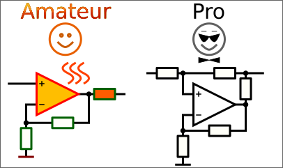
The easiest way to build a driver with specified output impedance is to use an amplifier with high load compatibility and add a resistor to its output. The penalty is voltage drop across this resistor, so there is power loss and we need a higher supply voltage. If our driver is able to deliver the same voltage and current to the same load, but the extra resistor will have a lower value, our device will be able to deliver the same output power at a lower supply voltage. Less power losses, less heat, and longer working time when a battery is used.
There is an idea how to solve this problem: active termination. We can synthesize the output impedance!
Now when we know what we want, go to design our drivers!
Single-Ended Driver
Maxim Integrated» engineers shared equations to design active termination single-ended drivers in [1]. The idea is to add positive feedback to reduce the output resistor value, use it to measure current, and synthesize the desired output impedance. As the result we have lower power losses. It is interesting that this circuit looks exactly as Improved Howland Current Pump! We just use another set of equations to get the desired behavior.
Let«s design single-ended drivers with parameters: gain G is 1 when unloaded, output impedance Zout is 50 Ohm. It means that if we load our driver with 50 Ohm resistor, the output voltage drops by half and gain is 0.5.
Inverting Active Termination Driver
Select Ro = 22 Ohm, which is much lower than 50 Ohm. Now we can choose either R1 or R2. Let«s choose R2 = 3 KOhm.
     Ro    22 Ohm
K = ———— = —————— = 0.44
    Zout   50 Ohm

     R2     3 kOhm
R1 = ——— = ———————— = 6818 ≈ 6.8 K (E24)
     K G   0.44 × 1
Now we need to choose R3, let«s set it to 4.3 kOhm.
R4 = R3 [(1 + K G)/(1 − K) − 1] = 4.3 KOhm × [(1 + 0.44 × 1)/(1 − 0.44) − 1] = 6757 ≈ 6.8 K (E24)
Enter the values into a simulator. The output voltage drops by half when 50 Ohm load is connected, so the circuit works exactly as expected.
Why are we wasting our time and money?
We had to do calculations and add 2 resistors. What are benefits?
Let«s compare an inverting driver and inverting active termination driver with the same parameters.
The output voltages, green and yellow lines, are the same 0.5 Vpp. But the common driver output voltage is 1 Vpp, the cyan line, and the active termination driver output voltage is 0.72 Vpp, the purple line. So the power losses of the common driver are:
P1 = Urms^2 / R = [√2 × (1 Vpp − 0.5 Vpp)]^2 / 50 Ohm = 10 mW
and for our active termination driver:
P2 = Urms^2 / R = [√2 × (0.72 Vpp − 0.5 Vpp)]^2 / 22 Ohm = 4.4 mW
More than 2 times lower! And lower supply voltage can be used.
Obviously, the lower the Ro value, the lower the power losses.
The Zout/Ro ratio defines the R1/R2 ratio and there is some output impedance of a used Op Amp. When the output is shorted to the ground, Ro acts as a protection. And the lower Ro value, the more the positive feedback must be, which can cause instability and distortions. So Ro should not be too low.
Thus, the most used Zout/Ro ratio in real circuits is about 2 and practical limit is about 10.
Attention, please! Lower supply voltage can be used only with a heavy load. If the driver works with light loads too, supply voltage must be high enough.
Choosing R3 and R4
We see that R3 and R4 are arbitrary values linked with the equation:
R4 = R3 [(1 + K G) / (1 − K) − 1] = R3 N
So what values to choose?
Maxim Integrates» engineers write in [1]:
Ensure that the time constant of the negative feedback loop dominates the overall loop control.
…
TC (−) = Ccom (R1 || R2)
TC (+) = Ccom (R3 || R4)
Set TC (−) < TC(+)
If we design two drivers with unloaded gain of 1 and 50 Ohm output impedance, take parameters from the OPA2134 datasheet, for example, we will see 2.2 dB peak at 2.8 MHz when (R1||R2) > (R3||R4), the top circuit and green line on the chart.
Stability check shows that the phase margin is about 40° for the top circuit and 84° for the bottom circuit.
Of course, a capacitor can be added in parallel with R2 to increase the phase margin.
R3 and R4 are connected in parallel with a load, so it is the reason to have them not too low. On the other hand, there is resistor thermal noise, which can be important if we design a driver for some audio device, for example, so their values should be as low as possible.
To solve this problem, a good start value for R3 is to be equal to R1.
Input Impedance of the Inverting Active Termination Driver
The input impedance of the inverting active termination driver without a load is:
                     R2 R3
Rin.unloaded = R1 − ———————
                    Ro + R4
and with a load is:
                            R2 R3 Rload
Rin.loaded = R1 − ——————————————————————————————
                  (Ro + R4) Rload + (R4 + R3) Ro
Thus, unlike the inverting amplifier, the input impedance of the drivver is less than R1 and depends on Rload. In our case Rin.unloaded ≈ 4.9 kOhm and Rin.loaded ≈ 5.7 kOhm with 50 Ohm load.
Pay attention that the output impedance of the previous stage can affect the driver parameters, though usually it is not a problem, because it is low.
Non-Inverting Active Termination Driver
AN-3390 [1] says:
Inverting only practical operation.
Still we will try to design the non-inverting version of the driver.
It is the non-inverting amplifier, so we can design the non-inverting active termination driver only with a gain greater than 1. The equations are the same but we must subtract 1 from specified unloaded gain value or 0.5 from a loaded gain value. If we enter the same values as in the previous example, the gain will be 2 when the driver is unloaded.
Our simulation confirms that at the same component values Gain = 2 when the driver is unloaded and 1 when loaded.
Input Impedance of the Non-Inverting Active Termination Driver
The input impedance of the non-inverting active termination driver without a load is:
                    R1 (Ro + R4)
Rin.unloaded = R3 − ————————————
                         R2
and with a load is:
                  R1 [(Ro + R4) Rload + R4 Ro]
Rin.loaded = R3 − ————————————————————————————
                        R2 Rload − R1 Ro
In our case Rin.unloaded ≈ −11.16 kOhm and Rin.loaded ≈ −8.3 MOhm with 50 Ohm load.
Yes, it is negative! It means that the current flows from the driver input, so the previous stage must be able to sink this current.
Fully Differential Active Termination Driver
Fully differential version of the driver is described in [2] in Chapter 16.
Let«s design a driver with the same parameters: gain is 1 when unloaded, output impedance Zout is 50 Ohm.
Select Ro = 16 Ohm, R2 = 3 KOhm.
        R2          3 kOhm
R3 = ———————— = —————————————— = 8.333 ≈ 8.2 K (E24)
         2 Ro       2 × 16 Ohm
     1 − ————   1 − ——————————
         Zout         50 Ohm
                2 Zout R2 R3                           2 × 50 × 3000 × 8200
R1 = ————————————————————————————————— = ————————————————————————————————————————————— = 4701 ≈ 4.7 K (E24)
     G [2 Ro R3 + Zout (R3 + Ro − R2)]   1 × [2 × 16 × 8200 + 50 × (8200 + 16 − 3000)]
Differential Active Termination Driver
Another variant is used in ADSL modems and described in [3], for example. Since it is a modified differential amplifier, there is limitation for minimum gain.
Let«s design a driver with parameters: gain is 2 when unloaded, output impedance Zout is 50 Ohm.
Select Ro = 20 Ohm, R2 = 910 Ohm.
        R2          910 Ohm
R3 = ———————— = —————————————— = 4550 ≈ 4.7 K (E24)
         2 Ro       2 × 20 Ohm
     1 − ————   1 − ——————————
         Zout         50 Ohm
                           2 R2 R3                                                    2 × 910 × 4700
R1 = ———————————————————————————————————————————————————— = ———————————————————————————————————————————————————————————————— = 4320 ≈ 4.3 K (E24)
     Ro − R2 − R3 + G (Ro + R3 − R2 + 2 R3 Ro / Zout) / 2   20 − 910 − 4700 + 2 × (20 + 4700 − 910 + 2 × 4700 × 20 / 50) / 2
The differential input impedance is constant, 2×R1.
Balanced Driver or Floating Differential Output
There is one problem with differential drivers described above: if one of their outputs is loaded to the ground, the other output voltage will not change, so the differential output voltage will be lower. But what if we want to have a constant differential voltage, as if it were a transformer?
We would like:
- Both outputs have the same output voltage with opposite phase;
- When one output is loaded to the ground, the opposite output increases output voltage, so the differential output voltage remains the same;
Single-Ended Input Balanced Driver
There are ready-made drivers: SSM2142, DRV134, DRV135, THAT1606, THAT1646.
They are pin-to-pin compatible, easy in use, but there are drawbacks too:
- Supply voltage is from ±4.5V to ±18V;
- Output impedance is fixed to 50 Ω;
- Limited bandwidth;
So if we need a driver with lower or higher output impedance or supply voltages, or higher bandwidth, we have to design our own driver.
We find such a driver initially in HP 8903A Audio Analyzer. The idea of its output circuit was published in [4] in 1980. There is a mistake in the circuit, U2» inputs must be exchanged.
Author«s recommendation:
R2/R1 = R12/R11, R3 = R7, R6 = R10, R4 = R5 = R8 = R9
R2/R1 = (2R6 + R4) / 2R3
There is a service manual of this device on the Internet, so we can get exact values and see how it worked. According [4] the parameters are: gain is 1.125, the output impedance of the driver is 480 Ohm, so 120 Ohm resistor is added to have the output impedance of 600 Ohm.
Our simulation shows that the driver has 600 Ohm floating differential output. If we load one output to ground even with 1 GOhm resistor, the output goes down like a transformer. But its outputs do not have signals with equal levels and opposite phases how we could wait.
The next version of the driver we find in 1995 in dbx168a [5] and in 1996 in dbx740X [6].
Simulation shows that this driver is balanced perfectly. dbx» engineers solved problems by changing resistor values, adding DC servo and load resistors. The gain is about 1.5, the output impedance is about 30 Ohm.
We find a new version in Behringer devices starting from about 2000 (sorry, I do not remember where I got it and you can find it in different devices).
Using a simulator we see that the unloaded gain is about 1, the output impedance is about 100 Ohm.
Now the driver works without an extra Op Amp and has good balance. So the problems were finally solved.
So, how does the driver work and how to design it if we want to change its parameters?
Of course, you have already realized that it is the inverting and non-inverting single-ended active termination drivers compiled in one driver.
We have seen earlier that it is not so easy to make a working driver using this circuit. It is because both legs are not equal.
The algorithm to design the balanced driver is:
- Calculate the Inverting and Non-Inverting Active Termination Driver with twice of specified gain and Ro = Zout / 2;
- Set (R3 = R5) = (2 R3 of the Inverting Driver) and (R6 = R8) = (2 R1 of the Non-Inverting Driver);
- Vary R3, R4, R5, R6, R7, R8 to get specified gain when unloaded and a half of the gain when loaded at the load equals to its output impedance; Then verify that both output voltages are almost equal;
- If you is not able to get the desired result, change Ro and start again;
Keeping in mind that (R3 || R5) ≈ (R3 of the Inverting Driver) and (R8 || R6) ≈ (R1 of the Non-Inverting Driver) you can do it manually using a simulator intuitively in about an hour varying resistor values. And if you set (R3 || R4 || R5)
Of course, a computer will do it much faster and better. Several variants can be computed to choose the best one.
Important note! This circuit is very sensitive to the resistor values, so it is better to use 0.1% resistors.
Differential Input Balanced Driver
Another idea of this driver is to use two similar drivers. But in this case we have differential input, so if we need single-ended input, an extra Op Amp must be added.
Let«s design balanced driver with parameters: gain G is 1 when unloaded, output impedance Zout is 50 Ohm. The equations are the same as for Inverting Active Termination Driver, but we need to change the gain and split R3» into R3 and R5.
Select Ro = 18.7 Ohm and R2 = 4.42 KOhm.
     Ro    18.7 Ohm
K = ———— = ———————— = 0.374
    Zout    50 Ohm

             R2      4.42 kOhm
R1 = R3' = ————— = ————————————— = 5909 ≈ 5.9 K (E48)
           2 K G   2 × 0.374 × 1

R4 = R3' [(1 + 2 K G)/(1 − K) − 1] = 5900 × [(1 + 2 × 0.374 × 1)/(1 − 0.374) − 1] = 10574 ≈ 10.5 K (E48)

R5 = R3' (1 + 2 G) = 5900 × (1 + 2 × 1) = 17800 ≈ 17.8 K (E48)

     R3' R5    5900 × 17800
R3 = ——————— = ———————————— = 8825 ≈ 8.66 K (E48)
     R5 − R3'  17800 − 5900
The circuit works, but an extra circuit is needed if the driver must have single-ended input.
This circuit is also sensitive to the resistor values, so it is better to use 0.1% resistors.
A bias can be added using some reference voltage at R3, but to make circuit output voltage DC stable, a DC servo is needed like in dbx» circuits.
Conclusion
Using active termination we can synthesize the output impedance and make our circuits more efficient, greener. Price for it is complexity and careful design.
References
- Maxim Integrated, Application Note 3390, Reduced Termination Loss by Active Synthesis of Output Impedance.
- TI, «Fully-Differential Amplifiers».
- TI, «Active output impedance for ADSL line drivers».
- Hewlett-Packard Journal, August 1980, p. 12, «Floating a Source Output» by George D. Pontis.
- dbx168a, Service Manual.
- dbx740X, Service Manual.
- «idealCircuit», a simulator.
- «Circuit Calculator», an electronics circuit design tool.
