[Из песочницы] Real-time edge detection using FPGA
Introduction
Our project implements a real-time edge detection system based on capturing image frames from an OV7670 camera and streaming them to a VGA monitor after applying a grayscale filter and Sobel operator. Our design is built on a Cyclone IV FPGA board which enables us to optimize the performance using the powerful features of the low-level hardware and parallel computations which is important to meet the requirements of the real-time system.
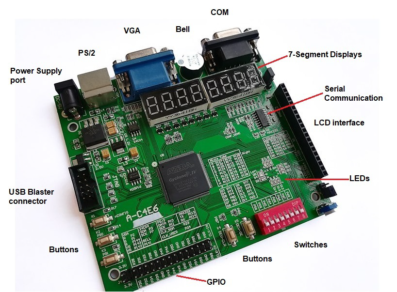
We used ZEOWAA FPGA development board which is based on Cyclone IV (EP4CE6E22C8N). Also, we used Quartus Prime Lite Edition as a development environment and Verilog HDL as a programming language. In addition, we used the built-in VGA interface to drive the VGA monitor, and GPIO (General Pins for Input and Output) to connect the external hardware with our board.
Architecture
Our design is divided into 3 main parts:
- Reading the data pixels from the camera.
- Implementing our edge detection algorithm (grayscale converter and Sobel operator).
- Displaying the final image by interfacing with a VGA monitor.
Also, there is an intermediate memory storage between reading/writing the data and operating on this data. For this purpose, we implemented two buffers that work as temporary space for pixels before they are used.
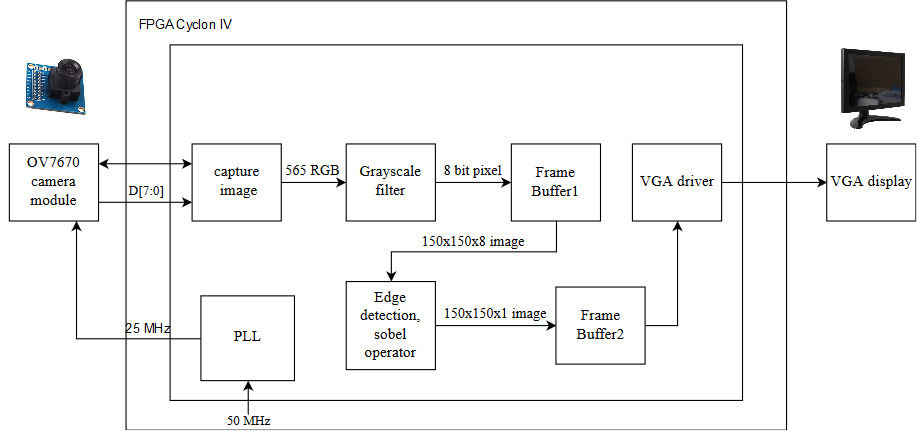
Note that after we took the pixel from the camera, we did not store it directly into the intermediate memory buffer. Instead, we converted it to the grayscale then we stored it in the buffer. This is because storing 8-bit grayscale pixels takes less memory than storing the colored pixels which are 16-bits. Also, we have another buffer which stores the data after applying the Sobel operator to make them ready to be displayed on the monitor.
Here are the details about the implementation of our architecture:
Camera
We used OV7670 camera which is one of the cheapest camera modules that we found. Also, this camera can work on 3.3V and does not need difficult communication protocols like I2c or SPI to extract the data of the image. It only requires SCCB interface which is similar to I2c interface to set the configuration of the camera in terms of color format (RGB565, RGB555, YUV, YCbCr 4:2:2), resolution (VGA, QVGA, QQVGA, CIF, QCIF) and many others settings.
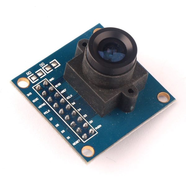
The video consists of frames which are being changed at a specific rate. One frame is an image consisting of rows and columns of pixels where each pixel is represented by color values. In this project, we used the default configuration of the camera where the frame’s size is the VGA resolution 640×480 (0.3 Megapixels), and the pixel’s color format is RGB565 (5 bits for Red, 6 bits for Blue, 5 bits for Green) and the rate of changing the frames is 30 fps.
In below, the connections of the camera to the FPGA using the GPIO which exists in the development board:
| Pin in the camera | pin in the FPGA | Description | Pin in the camera | pin in the FPGA | Description |
|---|---|---|---|---|---|
| 3.3V | 3.3V | Power Supply (+) | GND | GND | Ground Supply Level (-) |
| SDIOC | GND | SCCB clock | SDIOD | GND | SCCB Data |
| VSYNC | P31 | Vertical synchronization | HREF | P55 | Horizontal Synchronization |
| PCLK | P23 | Pixel’s clock | XCLK | P54 | Input System clock (25 MHz) |
| D7 | P46 | 8th bit of data | D6 | P44 | 7th bit of data |
| D5 | P43 | 6th bit of data | D4 | P42 | 5th bit of data |
| D3 | P39 | 4th bit of data | D2 | P38 | 3rd bit of data |
| D1 | P34 | 2nd bit of data | D0 | P33 | 1st bit of data |
| RESET (Active Low) | 3.3V | Reset pin | PWDN | GND | Power Down pin |
Note that we did not use SCCB interface for configuration. So, we put their corresponding wires on the ground to prevent any floating signals that can affect the data.
To provide the 25MHz clock for the camera we used Phase-Locked Loop (PLL) which is a closed-loop frequency-control system to provide the needed clock from the 50MHz provided from the board. To implement the PLL, we used the internal IP catalog tool inside Quartus software.
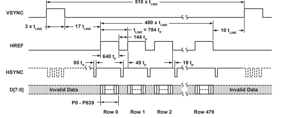
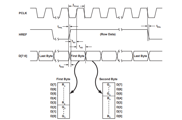
This camera uses vertical synchronization (VSYNC) signal to control the sending process of the frame and the horizontal synchronization (HREF) signal to control the sending of each row of the frame. This camera uses only 8 lines of data (D0-D7) to transfer the bits which represent the pixel’s color values as the camera divides the 16-bit RGB pixel value into 2 (8-bit) parts and send each one separately.
The below figures from the datasheet of OV7670 camera module illustrate the signals of vertical and horizontal synchronization.

Grayscale converter
To produce a grayscale image from its original colored image, many factors should be taken into consideration, because the image may lose contrast, sharpness, shadow, and structure. Moreover, the image should preserve the relative luminance of the color space. Several linear and non-linear techniques are used for converting the color image to grayscale. Accordingly, to achieve our objective we used the colorimetric (perceptual luminance-preserving) conversion to grayscale represented in the following equation:

To enhance the performance in terms of computations, it is faster to use the shift operator. Hence, the equation above can be reduced to the following:

As a result, after capturing a (565 RGB) pixel value from the camera, it can be immediately converted into an 8-bit grayscale pixel value applying the formula of conversion. The grayscaled image is easier to store in the memory and fast enough to serve the functionality of our real-time system as its complexity is approximately logarithmic and FPGA can make it even faster by accessing the memory in parallel. After that, the stored image is ready for implementing the edge detection algorithm.
Intermediate memory (The buffer)
We have 2 buffers, the first one is used to store the pixels after converting them to grayscale and its size (8-bits x 150×150) and the second one is used to store the pixels after applying Sobel operator and the threshold for the output value and its size (1-bit x 150×150). Unfortunately, 150×150 buffers do not store the whole image from the camera but stores only part of it.
We have chosen our buffers» size as 150×150 because of the limitation of cyclone IV memory as it only has 276.480 Kbit while our two buffers take 202.500 Kbit (150×150 x 9) which is equivalent to 73.24% from the original memory of cyclone IV and the rest of the memory is used for storing the algorithm and the architecture. Furthermore, we tried (170×170) as a size for our buffers which takes 94.07% from the memory which does not leave enough space implementing the algorithm.
Our buffers are True Dual-port RAM which can read and write in different clock cycles simultaneously. Here, we created our implementation instead of using the IP catalog tool inside Quartus software to have more flexibility in the implementation. Also, we integrated both buffers in only one module instead of having different modules.
Sobel operator
We used a first derivative edge detection operator which is a matrix area gradient operator that determines the change of luminance between different pixels. To be more precise, as it is a straightforward and efficient method in terms of memory usage and time complexity, we used Sobel gradient operator that uses 3×3 kernel centered on a chosen pixel to represent the strength of the edge. The Sobel operator is the magnitude of the gradient computed by:

Where Gx and Gy can be represented using convolution masks:

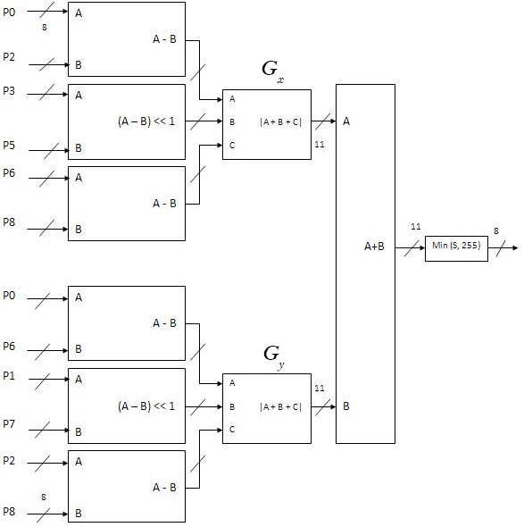
Note that the pixels that are closer to the center of the mask are given more weight. Also, Gx and Gy can be calculated as follows:

Where pi is the corresponding pixel in the following array, and the value of pi is 8-bit grayscale value:

It is a common practice to approximate the gradient magnitude of Sobel operator by absolute values:

This approximation is easier to implement and faster to calculate which again serves our functionality in terms of time and memory.
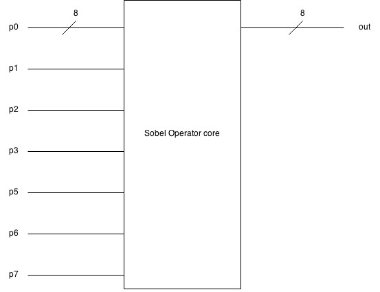
Here is the block diagram of Sobel operator which takes 9 (8-bit) pixels as input and produces (8 bit) pixel value:
And here is the detailed block diagram of the Sobel operator implementation.
VGA monitor
Our development board has a built-in VGA interface which has the capability to display only 8 colors on the VGA monitor as it has only 3-bits to control the colors through one bit for Red, one for Green and one for Blue. This has made our debugging harder as it prevents us to display the image from the camera directly to the monitor. So, we used a threshold to convert the pixels into 1-bit value so it is possible to display the image.
The VGA interface works like the camera as it operates pixel by pixel from the upper-left corner to the lower-right corner. Using the vertical and horizontal synchronization, we can synchronize the signals that control the flow of pixels.
The vertical synchronization signal is used to represent the index of the row while the horizontal synchronization signal is used to represent the index of the column. Also, both signals use front porch, sync pulse and back porch as synchronization signals to separate the old row from the new row in the horizontal synchronization signal, and the old frame from the new frame in the vertical synchronization signal.
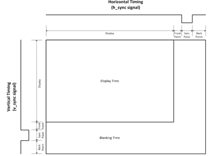
We used the standard VGA signal interface (640×480 @60 MHz). All the standard specifications of the signal is described here.
Testing
Before putting everything together and testing the real-time system. We first had to test each part separately. At first, we checked the values and signals that come from the camera by displaying certain pixel values. Then, with the help of OpenCV using Python programming language, we were able to apply Sobel filter on several images to compare the results with our algorithm and check the correctness of our logic. Moreover, we tested our buffers and VGA driver by displaying several static images on the VGA monitor after applying Sobel operator and thresholding. Furthermore, by changing the value of the threshold, the accuracy of the image is affected.
The python code which we used:
# This code is made to test the accuracy of our algorithm on FPGA
import cv2  #import opencv library

f = open("sample.txt",'w')  # Open file to write on it the static image initialization lines
img = cv2.imread('us.jpg')  # Read the image which has our faces and its size 150x150
gray = cv2.cvtColor(img, cv2.COLOR_BGR2GRAY)        #convert to grayscale
sobelx = cv2.Sobel(gray,cv2.CV_64F,1,0,ksize=3)     #x-axis sobel operator
sobely = cv2.Sobel(gray,cv2.CV_64F,0,1,ksize=3)     #y-axis sobel operator
abs_grad_x = cv2.convertScaleAbs(sobelx)
abs_grad_y = cv2.convertScaleAbs(sobely)
grad = abs_grad_x + abs_grad_y

for i in range(0,150):
    for x in range(0,150):
        #read the pixels of the grayscaled image and Store them into file with specific format to initialize the buffer in FPGA code
        f.write("data_a[{:d}]<=8'd{:d};\n".format(i*150+x,gray[i][x]))
        #apply threshold to be exactly like the code on FPGA
        if(grad[i][x] < 100):
            grad[i][x] = 255
        else:
            grad[i][x] = 0

cv2.imshow("rgb", img)  #Show the real img
cv2.imshow("gray",gray) #Show the grayscale img
cv2.imshow("sobel",grad)#Show the result img
cv2.waitKey(0)          #Stop the img to see it
Results
As a result of our implementation, we got a real-time edge detection system that produces a 150×150 image after applying the grayscale filter and Sobel operator. The implemented system provides 30 fps. The camera runs on a 25MHz clock and the system, in general, meets real-time deadlines without noticeable lag. Moreover, the threshold value can affect the amount of details and the noise in the final image.
Here is a comparison between Sobel operator on FPGA and OpenCV sobel operator:
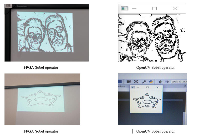
Below is an illustrative video of the results:

Here is the link of the repository on Github which has all the source codes.
Future improvements
As we are using FPGA Cyclone IV, we are limited to its memory capacity and the number of logic gates. Hence, as a future improvement, we can use an external memory source or we can implement our work on another board so we can display all the pixels from the image received from the camera.
Furthermore, although Sobel operator is fast and simple to implement, it is noticeably sensitive to noise. To eliminate the produced noise, we can use a noise filter like the non-linear median filter which works perfectly fine with our system if we had enough memory to implement a third buffer. This will produce a smoother image with sharp features removed.
Accordingly, we used the built-in VGA interface of the FPGA that can only produce a 3-bits image. Thus, we couldn«t display the grayscaled image as it needs 8 bits to be displayed. As a result, implementing another interface or using more powerful board will enhance the flexibility of displaying the image.
Conclusion
We were able to use our knowledge and understanding of crucial concepts in embedded systems as state-machines, computations parallelism, and hardware-software interfacing to create an efficient edge detection application that meets our objectives.
Acknowledgment
This project is built by a team consisting of two students: Hussein Youness and Hany Hamed in first year bachelor of Computer Science in Innopolis University in Russia.
This project is part of Computer Architecture course Fall 2018 in Innopolis University.
References
