System in Package, or What's Under Chip Package Cover?
Transistor feature size is decreasing despite constant rumors about the death of Moore«s law and the fact that industry is really close to physical limits of miniaturisation (or even went through them with some clever technology tricks). Moore«s law, however, created user«s appetite for innovation, which is hard to handle for the industry. That«s why modern microelectronic products aren«t just feature size scaled, but also employ a number of other features, often even more complicated than chip scaling.
Disclaimer: This article is a slightly updated translation of my own piece published on this very site here. If you’re Russian-speaking, you may want to check the original. If you’re English-speaking, it’s worth noting that English is not my native language, so I’ll be very grateful for the feedback if you find something weird in the text.
I«ve intentionally said «microelectronic product» instead of just «chip», because this article is about System in Package (SiP) technology allowing to connect many chips inside the single package.
The term System in Package is a way less popular than System on Chip (SoC) term, which is routinely used by every semiconductor company, and for a good reason as almost any modern chip is somehow a system with many functions fused together. The times of abundant chipsets are long gone, as the advantages of SoC are clear: less packages on the PCB, less area (read «cheaper»), less parasitic capacitances and inductances (read «faster»), easier to implement and use, cheaper to design and manufacture a single complex chip than a bunch of more specific ones.
But nothing is for free, and SoCs obviously have some downsides.
First, while trying to put all the pieces together, you are at risk getting a chip too big to fit into any package or, even worse, into the window of photolithographer. The latter restriction can be surpassed, but it«s almost always unreasonably expensive (with photo cameras being the most notable exclusion).
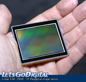
Here is Kodak Kaf39000 image sensor, it has area of 2000 square millimeters, and it uses mask stitching. The biggest non-stitched chip is NVIDIA Volta of 815 square millimeters, which is just 20 millimeters less that the largest possible size.
Second, the larger the chip is, the lower the yield, as any single speck of dust can ruin your day. And guess what? Lower yield means higher price.
Third, if your system contains heterogeneous components, like processor core, DRAM, and RF module, combining them together may be technologically impossible or, again, unreasonably expensive. For example, DRAM cells require specific high-density capacitors, and silicon-based RF circuits may be just worse than their counterparts produced on various A3B5 material (GaAs and likes). Even simple combination of digital processing and analog signal conditioning on the same chip creates significant noise problems. And I don«t even say about the fact that 180 nm ADC would easily be two orders of magnitude cheaper than adding its 14 nm analog to the 14 nm MCU chip.
The combination of all the factors above led to the change of trend from «we-will-pack-everything-into-the-single-chip» to more pragmatic approach — and to the fast development of various packaging technologies.
Performance and yield
The first example that comes into mind is recent rebirth of AMD, widely recognised as the result of their success with multi-chip systems (also helped by Intel«s troubles with yield on enormous 10 nm chips).
Pictured above is Intel«s 28-core Xeon. Chip area of this processors may reach crazy 456 square millimeters, while the maximum size of AMD chips is just 200 square millimeters for eight cores, their manycore products are actually two-layer PCBs with up to four dice inside the package.
This figure shows the PCB inside EPYC and Threadripper processors. In case of 16-core Threadripper, we still have four chips, but half of the cores are disabled. Why not just to use two dice instead? Or use smaller four-core dice?
First, having a single chip for all purposes is obviously much cheaper that designing a family.
Second, the same is true for PCB, packages, etc. It«s easier to disable excessive parts than to design a family of products.
Third and probably most important, yield of 200-sq.mm. die is still far from 100%, and disabling some already nonfunctional cores is a good way to use these defect dice. Intel does the same with their defect dice, but their yield problems are more severe due to larger chip area.
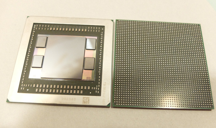
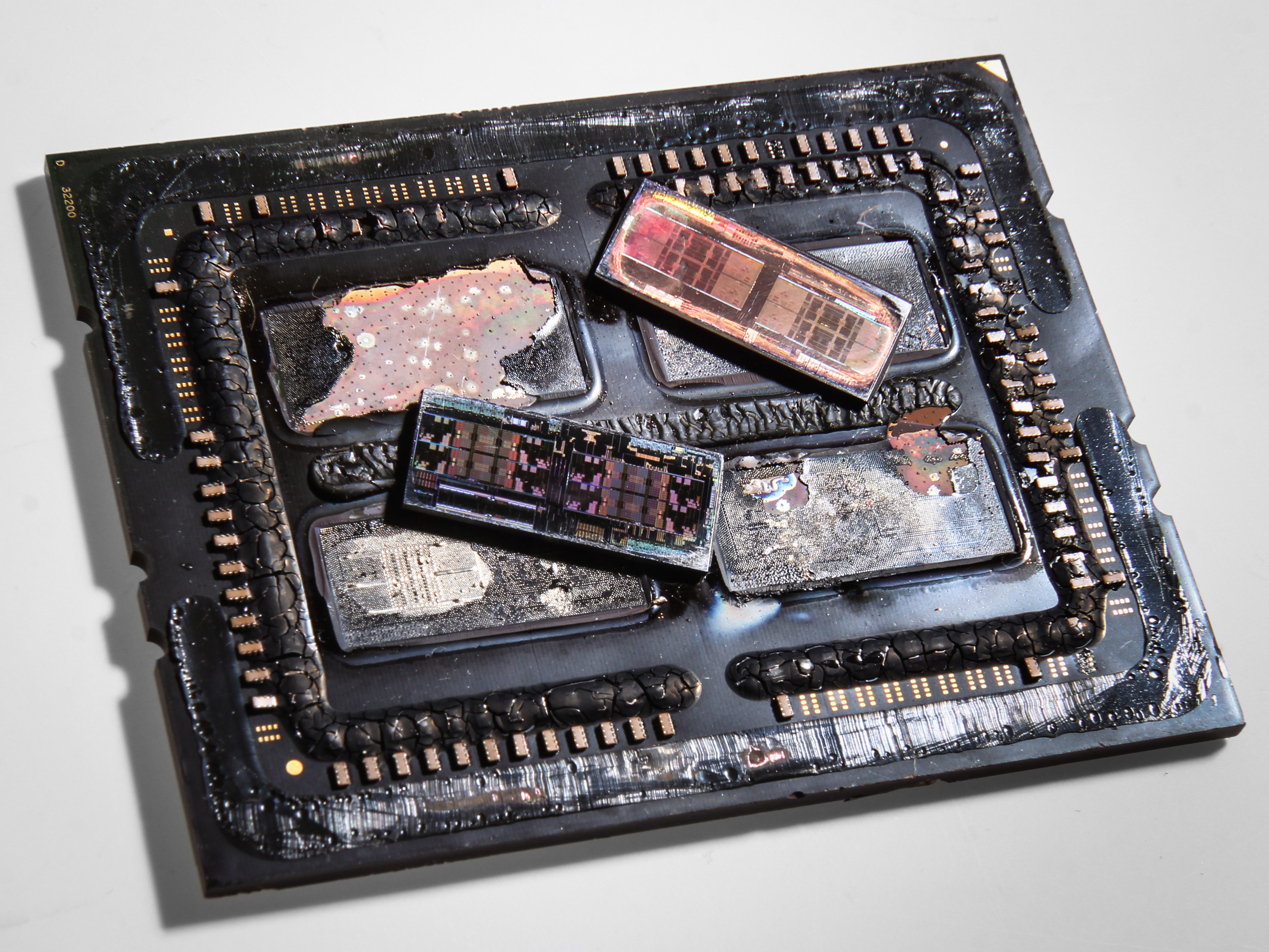
Here we have even more interesting example, again of AMD. Fiji is a GPU with embedded high-speed memory placed inside the package.Why is it important? Because shorter signal lines allow achieving higher speed and therefore higher performance. Putting different chips together makes the the difference between this and the previous example. It«s by the way not five dice inside as one may have suggested, but twenty two! Let«s look at the cross section:
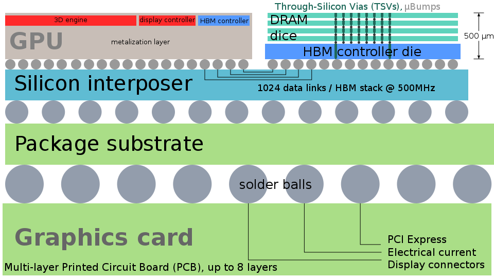
The upper level is GPU die itself and a stack of four memory dice connected by so called TSV (through-silicon-vias) — conducting contacts piercing the whole chip.
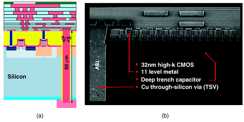
That«s how TSV looks like.
TSV technology was created for memory (one can«t have too much memory, right?), but it«s widespread now, partially thanks to the die laying under GPU and memory.
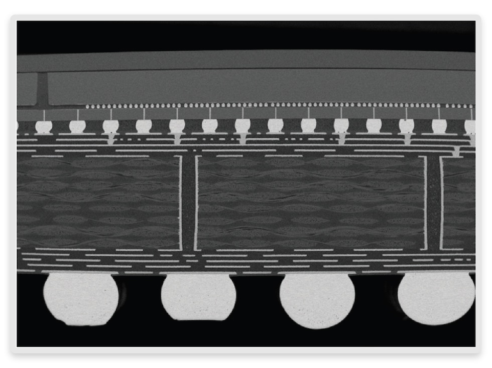
The die is called Silicon Interposer and it is a substitute for PCB made of silicon with a few (or many) levels of metallization, and with TSV. These interposers exist to connect multiple chips above them with a package substrate. Silicon technology allows having smaller feature size than any PCB (down to a few microns), but such it would be considered very simple and cheap for a silicon technology. Smaller feature size and TSV mean better performance than any PCB can provide, while yield will be very high. Interposers (alongside MEMS) are very interesting and important market, especially as they also allow reuse of old equipment for 200, 150, and even 100 mm wafers.
By the way, can you spot a mistake in the figure above?
Xilinx is another pioneer of 3D-integration. Their products are close to AMD«s ones (especially products carrying significant amounts of memory), and for the same reason. FPGA is a market where early switching to smaller process node can provide enormous advantage over competition. Decreasing chip size three to four times is said to provide two or three times yield increase at early stages of process node lifetime, from 20 percents to more than half. Moreover, FPGA is a complex, but regular structure, nearly ideal for investigating a large spectrum of manufacturing problems. This makes FPGA vendors the best early bird clients for fabs, and such a collaboration is fruitful for both parties: fab gets a great test chip while vendor is able to outrun the competition for at least few months.
Here we can see an FPGA from Xilinx. Upper die is a FPGA part with tons of 40 micrometer contacts to intermediate die called interposer. The lowest is a package, which has a dozen of its own metal layers.
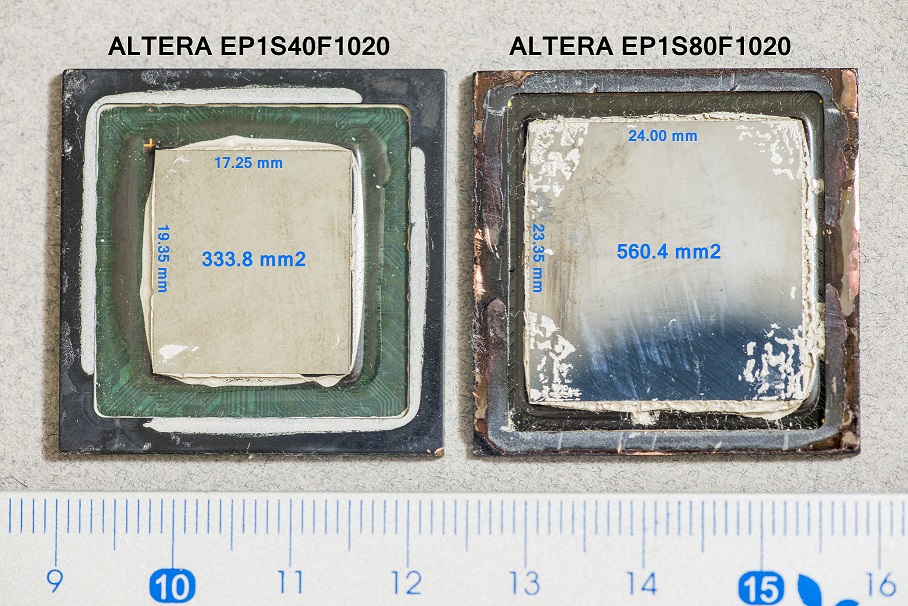
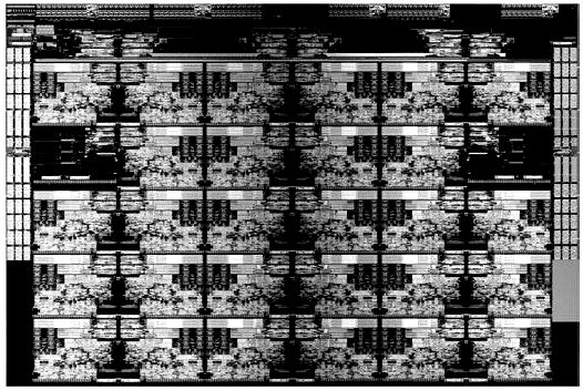
Enormous Altera FPGA die for the comparison. Five hundred and sixty square millimeters! If you see process engineers around, take care of them, there is a risk of heart stroke.
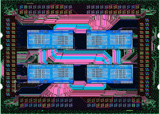
Intel/Altera obviously doesn«t just stare on competitors» progress. Here is their fresh SiP solution called EMIB (Embedded Multi-Chip Interconnect Bridge). A good example is Intel Stratix 10 FPGA.
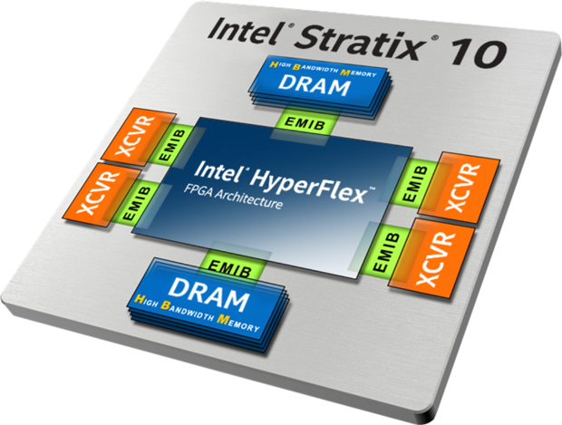
EMIB connect a FPGA die (still just one though), memory dice, and periphery dice. What«s EMIB? Typical interposer is much cheaper that «computational» die of the same size as interposer uses much larger process node; however, interposer is still enormous and therefore it«s reasonably expensive. Can one make it smaller?
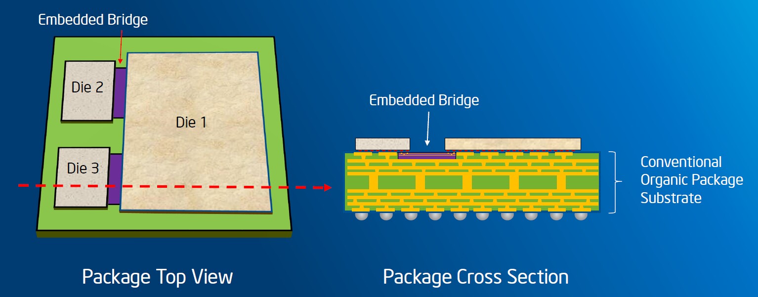
Intel«s answer is «yes we can». The idea behind EMIB is to use a few small interposers instead of a single large one, and integrate them into the package.
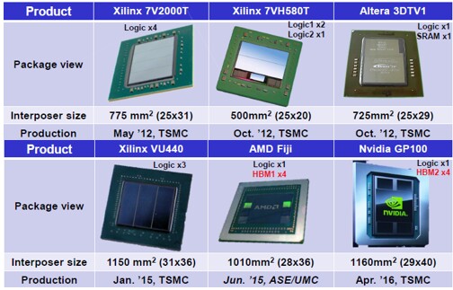
Here is a small gallery of products created with interposers. Look how enormous they are, and how Xilinx are created from pieces.
More than just performance
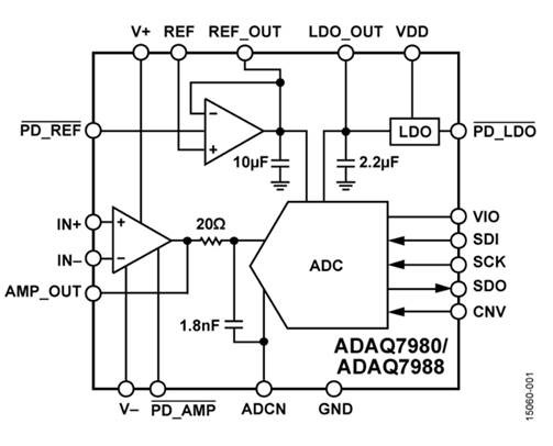
Figure below is Analog Devices» ADC and a schematic diagram. Looks like your typical PCB, just smaller, right? Yes, it is a PCB, but use of bare dice instead of packages allows to decrease parasitics and their influence on performance. The fact that the whole board was designed in Analog Devices also adds a layer of protection against system design mistake and leads to better user experience.
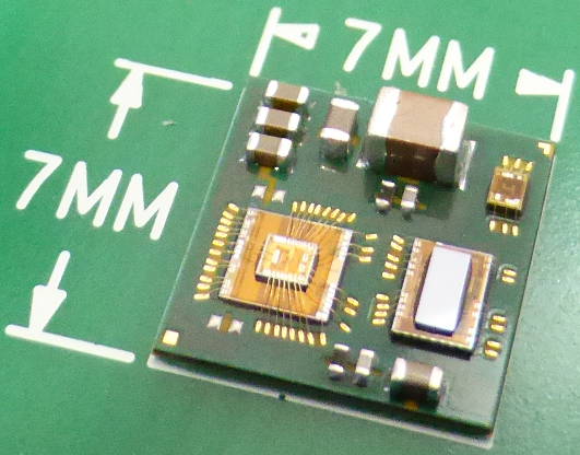
There is also a trick: do you see two dice packaged one over other? The higher one integrates active components (transistors) of ADC and probably of a dual operational amplifier, while the lower die consists of passives (resistors and capacitors). Placing passives onto separate die allows making them much bigger and therefore decrease parameter variation without making main die bigger and more expensive. Decreasing of parameter variation influence on analog circuit performance is a very big deal, and this move achieves cheaply.
Everything could be done on a single die (and is often done, especially on embedded ADCs), but such a die will be bigger (which could mean «more expensive«and «with lower yield»), and the technology must support all the necessary options (which also means «more expensive» due to larger number of masks). Moreover, when you combine many heterogeneous blocks on the same chip, you have to deal with their cross-influence. Digital noise influence on analog parts is probably the most important, but not the only one.
Package«s additional functionality
As we«ve seen before, packaging can make the product cheaper and even improve it. But what if we use package as a meaningful part of the product?
Intel realized so called FIVR (Fully Integrated Voltage Regulator) in their Haswell microprocessors. The aim of FIVR is to convert relatively high input voltage (1.8 V) into low and real´time controllable core supply voltage. Active components were on-chip, while passives (capacitors and inductances) were incorporated into processor package.
Integrated inductance is a headache of chip designers, because it«s bad, big, and with low inductance. They are used in radio-frequency chips, but there is almost no possibility of power transfer. Intel solved the problem by integrating dozens of small inductors into processor package. These inductors are working at 160 MHz without ferromagnetic cores. Doing so, Intel significantly simplified supply requirements for their device.
However, Intel ultimately scrapped FIVR, and reverted to more traditional supply approach for newer generations. There were some rumors that FIVR can be back, but in the end they were just rumors.
One of other options for integrating passives into package is LTCC (low temperature cofired ceramic). There are some limitations and issues (like limited nominal values and precision), but this technology is actively developed. Multilayer LTCC package looks like this:
All types of passive components are represented here, even metal heat sink (it«s a package for power RF IC). One can say that it«s not just a package, but a mix of package and ceramic PCB, these things are very popular for RF circuits and relatively cheap in small quantities.
What else?
There any many potential applications for systems in package, and it«s impossible to list them all. It«s also worth noting that they are significantly cheaper that new process nodes, which drives their commercial attractiveness.
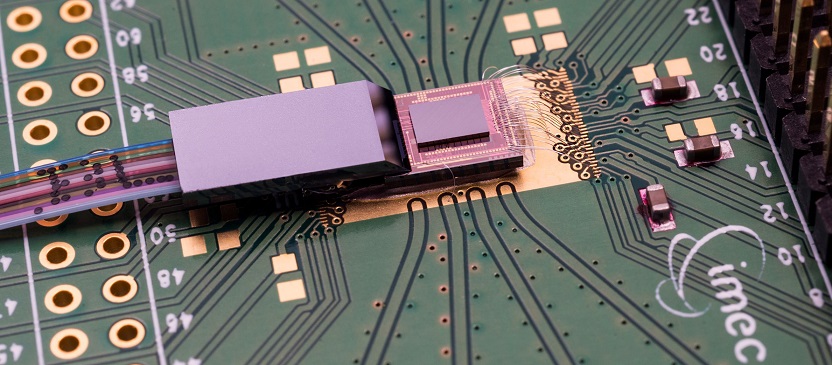
Optoelectronic systems are the last but not least example for this article. Ability to combinate optical receiver or transmitter (often built on compound semiconductor) with silicon supply and control chips is very promising. Picture below is a prototype of 400 Gbit/s (and 1 Tbit/s is promised for the future) optical lnk designed in IMEC.
There are also countless other applications like interposers with integrated capillaries for water cooling (not just for gaming and mining, but also for power switches and lasers), integrated MEMS and only God knows what else. And obviously we can«t escape the ubiquitous Internet of Things, where small size, low losses and ability to integrate radio and computational blocks together are all-important.
Chip package is believed to be the next big step in microelectronics by many, and we will likely see a lot of bright ideas in the nearest future.
