Building set for embedded developer
In this article I will talk about my attempt to create flexible, compact and beautiful modular prototyping framework
Introduction
I think many readers have used microcontroller-based development boards to prototype devices under development and to start debugging embedded software at a stage when a full-fledged device board is not yet ready. You can connect all the necessary peripherals to such boards with wires and start developing the firmware. But often such debug stands are terribly inconvenient, they take up a lot of space on the table, they are flimsy and not so easy to move from place to place, and the connections between the boards are unreliable.
In this article, I’ll show you how I try to solve these problems in my free time by developing my own flexible, compact and beautiful modular design for desktop prototypes.
The modules have not yet been made in hardware, so I prepared several 3D visualizations to dilute the text of the article with them. Well then, let’s get started…
Design
I have always wanted to use small modules. As much as possible and reasonable in terms of placing the components of a complete functional assembly on them. Ideally 50×50mm or even smaller.
The electrical connections between the modules must be reliable, the modules must be securely fastened together so that the rack does not fall apart from the next careless movement at the table and the contacts should not fail.
How to provide connections between modules?
Well, for example, module boards can be connected with connectors on the sides, laying them in one plane. But such an assembly will take up a lot of space and be vulnerable to bending. It is also problematic to make connections between modules along 2 axes, and all connectors for external connections will have to be brought up or down. Not a very good solution.
I can try cascading the module boards vertically, and the inter-module connectors can be placed at the top/bottom. The pinout of the connectors at the bottom and top is the same, all modules are paralleled on a common bus. Connectors for external connections can be placed on the sides. In this case, it is possible to mechanically fasten the modules using brass stands.
As a result, I came to this module PCB format:
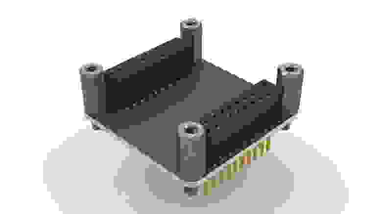 Module format
Expanding the assembly vertically is, of course, good. But expansion in the horizontal plane is still necessary, otherwise, with a large number of modules, we will get a narrow and unstable rack of modules. Horizontal expansion is also possible using hub boards. In one of the tiers, a larger hub board is placed, which is a multiple of the module dimensions (for example, 2×1, 1×2, 2×2, 3×2, etc.). It has all the same inter-module connectors at the top and bottom and mounting holes as conventional modules. Such hubs allow you to parallelize modules from several racks and connect them mechanically.
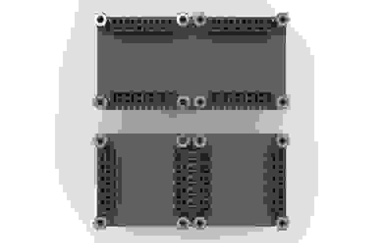 HUB_2×1 и HUB_1×2 modules
The obvious disadvantages of this solution are: the hub board consumes 1 tier in the assembly, and the mechanical connection between the racks is much lower than in one rack without hubs.
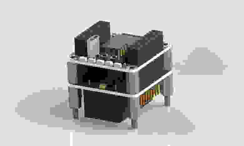
Design V1
Before I continue, I want to show you an intermediate design for which I even traced several modules.
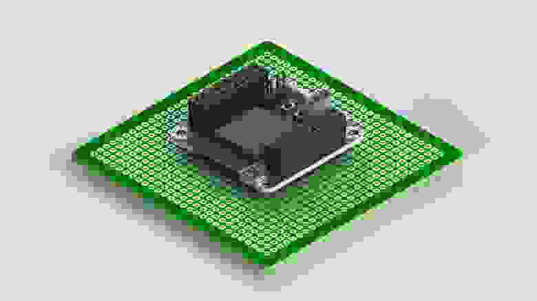
 The first version of the CPU module with dimensions of 42×42 mm
It uses 42×42mm boards. For inter-module connections, I used 4 connectors (1×11, female) on the top and 4 connectors (1×11, male) on the bottom. Step — 2.54 mm. This design had many problems and I don’t even know why I didn’t see them right away. For example, tricky rules for connecting modules. In order to be able to bring external connectors to the side, I planned not to use 1 (out of 4) intermodule connector (front and rear connectors duplicate each other). These modules use only front/rear connector pins, so the module can be rotated 180 degrees and still work. But that just confuses everything.
1-row connectors had low strength, and 1-row surface-mount females could not be found at all. As a result, it was proposed to solder the upper connector first, cut off the pins sticking out from below, and then solder the connector from below. But in this case, the quality of the soldering of the upper connectors will be poor, the connection of the lower connectors to the board will be poor, and the manufacturability of the module assembly will be poor.
All in all, this is a very bad design.
Design V2
This is the version that we are considering in detail today. Features:
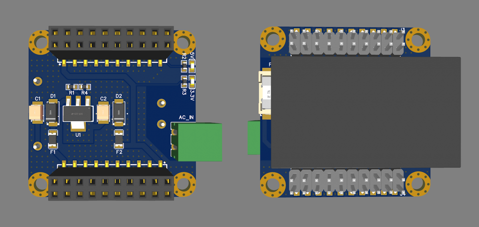
Module board dimensions — 40×40 mm. The corners of the board are rounded with a radius of 6 mm, which allows you to make a similar rounding in the device case.
For inter-module connection, 2 connectors 2×10 with a pitch of 2.54 mm are used. Surface mount connectors. Moms on top, dads on the bottom.
Inter-module connectors determine the distance between the boards of two adjacent tiers — 12 mm. Brass stands of this height are common and inexpensive. The stands are optional because the inter-module connectors hold the modules together quite well.
Connectors for external connections, controls and indications can be output from the front or rear.
The distance between the pins of the two inter-module connectors is a multiple of 2.54 mm pitch, so the bottom module can be inserted into an arbitrary size breadboard and soldered there. Or solder 2-row connectors on the breadboard and insert the bottom module into them. This allows you to neatly expand the assembly of modules using standard breadboards:
 Module soldered to breadboard
Modules placement in the case
Connectors for external connections are located with a 2 mm protrusion beyond the board. This is necessary so that the connectors of the device are not recessed into the case and do not stick out of it. A case with a wall of 1.6 mm can be printed on a 3D printer, the remaining 0.4 mm is the gap between the board and the wall of the case.
Brass stands used for fastening the modules to each other can also be used to fasten the assembly of modules in the case. The M3 screw can be used to fasten the module rack to the chassis. Another option is to use M3 injection nuts:

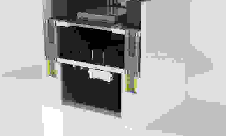
then the first level module is applied, the first level stands are screwed in, the second level module is applied, etc. In a cut it looks like this:
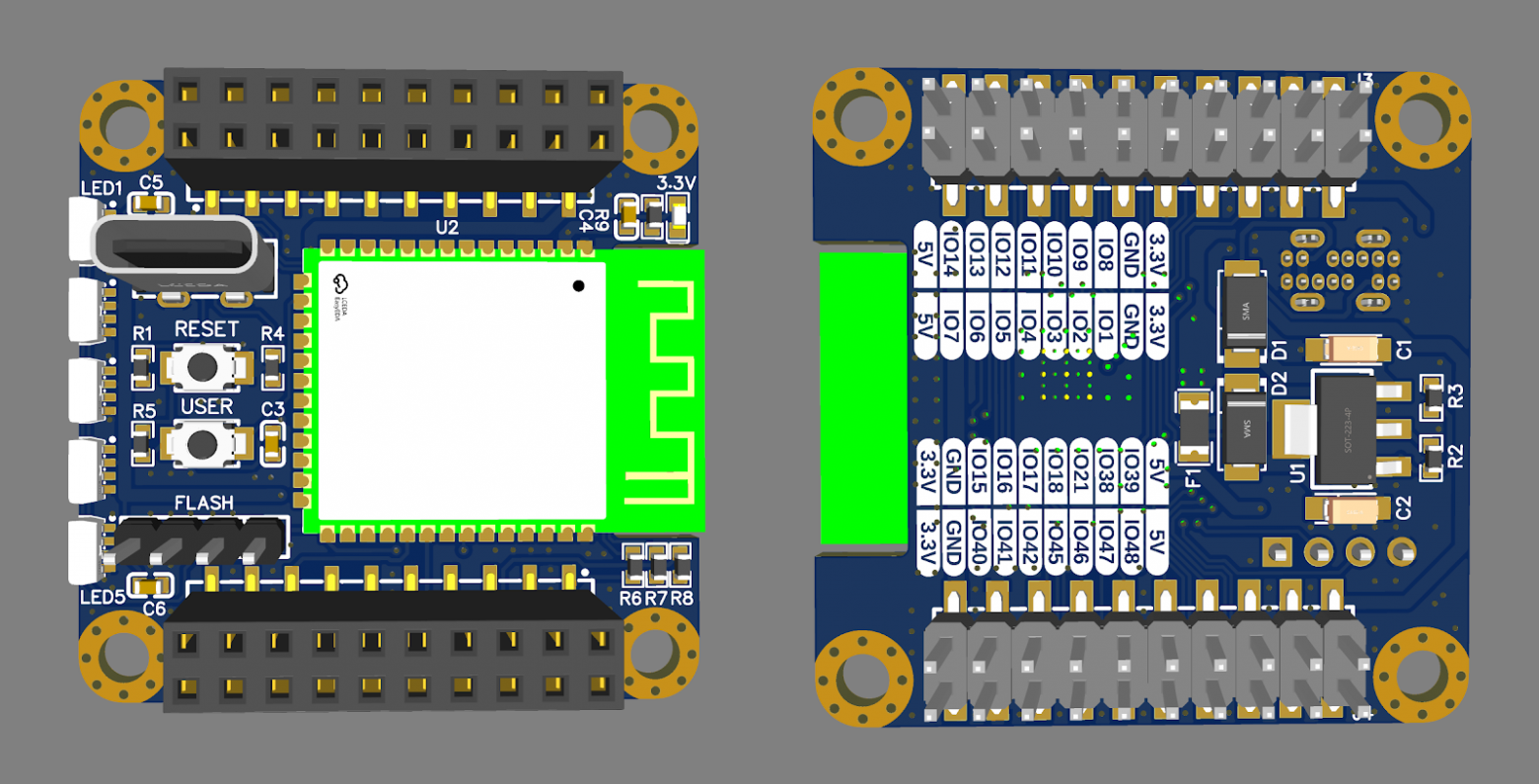
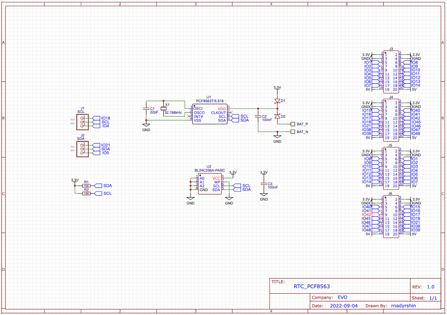
Pinout of intermodule connectors
The task of choosing the pinout of a common bus in a modular design is very non-trivial. If you forget to distribute some important signals among the pins, then in the future you will either have to put up with it, or redesign some of the modules (or even everything!).
But let’s take it step by step…
Inter-module connectors are located symmetrically and mechanically nothing prevents connecting the next module by turning it 180 degrees. This, in my opinion, is more bad than good. I’ve tried using this feature when designing modules, but it’s confusing most of the time.
However, if connected incorrectly, nothing should definitely burn out. Therefore, the pins responsible for supplying power are located so that, in any orientation of the module, power is supplied correctly.
Also, as you can see from the pinout, 2 supply voltages 3.3V are used as the main and 5V, which, in the future, some future modules will need (possibly).

There are still 28 pins left, which are marked in blue and green in the illustration above. Blue can be used as discrete or analog, green can only be used as discrete.
I am focusing on the ESP32-S3 microcontroller, the pin names in the pinout are taken from the documentation for it, which does not at all exclude the use of other microcontrollers in CPU modules.
ESP32-S3 is a powerful and modern microcontroller that has an interesting feature — the connection of the GPIO chip legs to the digital signals of the internal peripheral modules of the microcontroller can be done through a software-defined matrix (GPIO matrix). For example, the CAN_TX and CAN_RX signals can be connected inside the microcontroller to any of its external IO pins.
But this does not apply to analog inputs. 10 ADC1 channels are connected to pins IO1…IO10 and these channels cannot be connected to any other pins of the microcontroller. Another 10 ADC2 channels are connected to IO11…IO20 pins, but I do not plan to use ADC2, because, according to the documentation, ADC2 may fail with an error when WiFi is on. Therefore, pins IO1-IO10 can be used as analog inputs.
Unfortunately, all this does not simplify the task of distributing interface signals over 28 signal pins of intermodule connectors.
I chose the following approach — I distribute interfaces to pins gradually as modules are developed.
Now, for example:
pins IO1…IO10 are reserved for analog channels (their use for digital interfaces is possible, but may conflict with analog modules in the assembly);
pins IO18 (SCL) and IO21 (SDA) are reserved for I2C, which is supposed to connect a wide range of microcircuits and sensors — this is the main interface for low-speed nodes;
pins IO11 (SCLK), IO12 (MOSI), IO13 (MISO), IO14 (CS1), IO15 (CS2), IO16 (CS3/CE1), IO17 (CS4/CE) are reserved for SPI connection of communication chips and radio modules;
pins IO38 (SCLK), IO39 (MOSI), IO40 (MISO), IO41 (DC), IO42 (CS) are reserved for connecting displays via SPI.
All other pins are free for now.
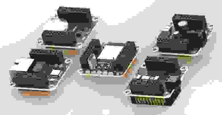
Developed modules
I should warn you that modules have not yet been made in hardware. So this is all just sketches. However, I can tell you a few interesting details about them.

While developing them, I tried to follow a few rules so that the assembly from modules was beautiful and convenient:
Connectors for external connections are located on the front or rear side of the module in accordance with where their location on the device is most convenient and logical. In those rare cases when you need the ability to turn the module 180 degrees, this feature is implemented by jumpers on the module board (or, if the opposite pins are not used in the assembled configuration, then it is enough to change it in the software).
I place connectors and indicators of the same type of modules (for example, PSU modules) in the same places.
I try not to place components at the bottom. Firstly, this will not allow them to be soldered automatically during production. Secondly, it increases the likelihood of conflicts in the location of the components of two adjacent tiers.
Most of the chip components are 0603 format. They are quite compact, but not yet too much for manual assembly.
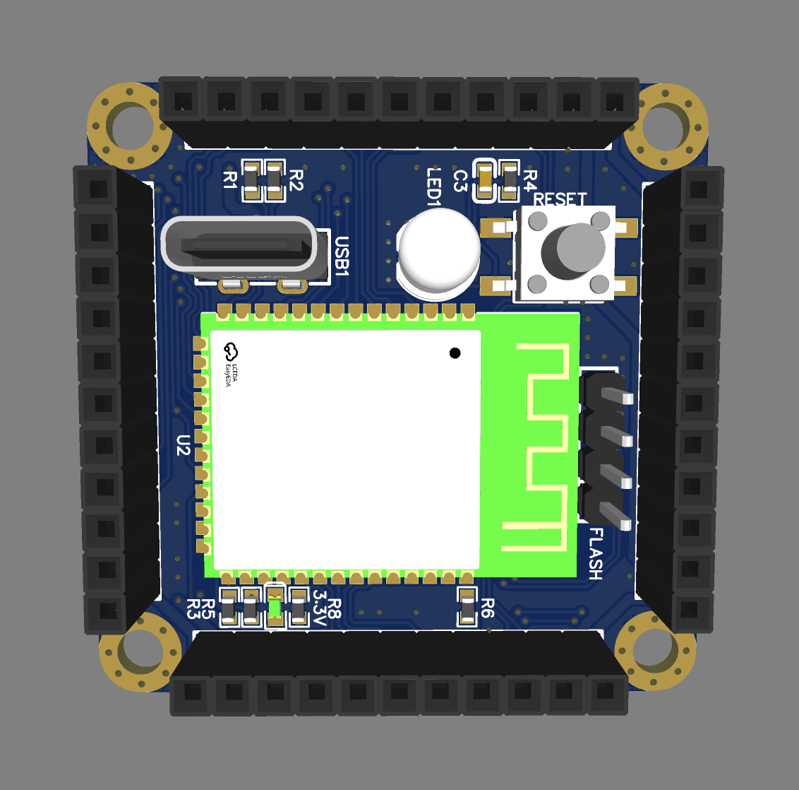
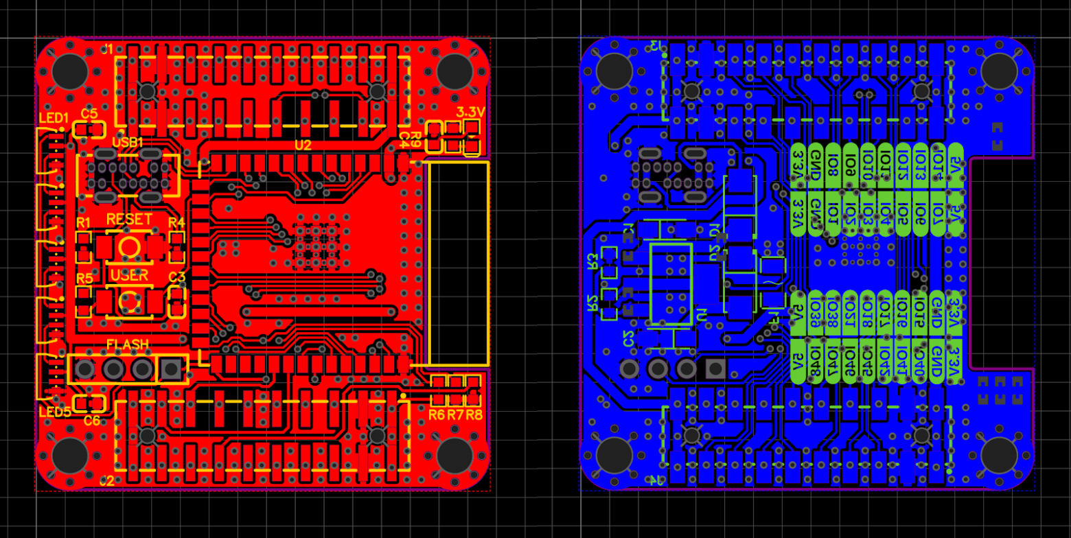
CPU_ESP32S3 module
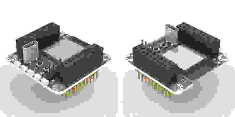 CPU_ESP32S3 module
The module is based on the ESP32-S3 microcontroller from Espressif, which was introduced in early 2022. This is the most sophisticated microcontroller in the modern Espressif product line, which is an update to the ESP32, which appeared in 2016 and is more or less known to developers and distributed.
If we compare them, we can see the following improvements in the ESP32-S3:
2 main microcontroller cores updated (Xtensa LX7 instead of LX6). The CoreMark test shows an 18.8% speed increase over the ESP32 at the same clock speed. Support for vector instructions has been added.
When connecting SPI flash (firmware memory) and SPI PSRAM (external pseudo-static RAM), 8-bit Octal SPI is now supported, which should give almost 2x speed increase with these chips compared to 4-bit Quad SPI in ESP32.
Uses QFN56 package instead of QFN48. The number of GPIOs has increased from 34 to 45, although the Octal SPI mentioned above takes up an additional 4 GPIOs. Finally, the limitations in some GPIOs have disappeared (for example, pins IO34 … 39 in ESP32 could only be used as inputs).
1 x USB Host/Device added. The USB PHY is built into the microcontroller. Device can only work as USB serial or JTAG.
LCD controller with hardware support for i8080/moto6800 parallel interface and RGB interface added.
A parallel DVP interface for connecting cameras has been added.
Bluetooth LE updated to version 5 (was 4.2) + Bluetooth mesh support added.
There are also disadvantages:
Ethernet MAC removed.
DAC removed.
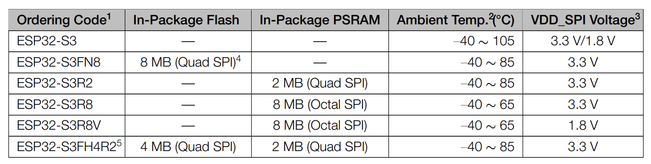
The ESP32-S3 chip can be equipped with a Quad SPI flash drive and a Quad/Octal SPI PSRAM. At the time of writing, Espressif offers the following options:
I don’t plan to solder the ESP32-S3 chips to the CPU_ESP32S3 module PCB. Instead, one of the modules that Espressif sells (with a built-in antenna or with an antenna connector) will be soldered:

I plan to use ESP32-S3-WROOM-1-N16R8 and ESP32-S3-WROOM-1U-N16R8. These are modules with a 16 MB QuadSPI flash and an ESP32-S3R8 chip (with 8 MB Octal SPI RAM inside the chip).
What else is on the CPU_ESP32S3 PCB:
USB-C connector (as a USB-Device port with the possibility of in-circuit debugging via JTAG through it). The connector is pointing up, so the module in the assembly must be located in the top tier if you want to connect to it.
The entire assembly of modules can be powered through the USB-C port. 5V from the USB-C connector is fed through the Schottky diode to the 5V bus (dropping to 4.8V). The 3.3V voltage is generated by the AMS1117-ADJ linear regulator. Its output voltage is set to 3.5V, which, through a Schottky diode, enters the 3.3V bus. Diodes are needed to decouple the power supplies of the assembly (there may be several).
4-pin connector — for flashing using an external USB-UART.
2 buttons: reset button and user button.
On the front there are 5 controllable RGB LEDs (Worldsemi WS2812B-4020) with a side glow orientation.
Rear right LED-indicator of 3.3V power supply.
In the next revision, I plan to remove the 4-pin connector and move the 3.3V regulator to the top side of the board (perhaps replacing the AMS1117 with something switching and more compact).

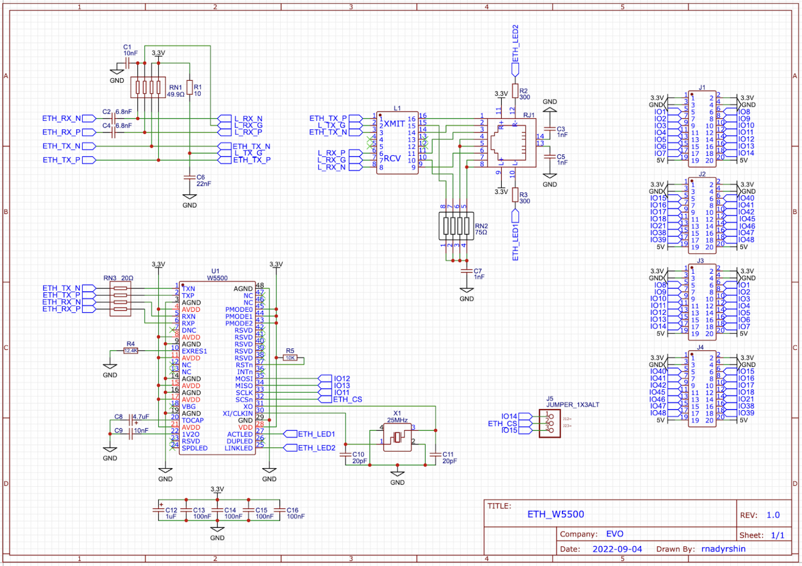
ETH_W5500 module
The ESP32-S3 does not have an Ethernet MAC, so the module uses the popular WIZnet W5500 TCP-IP controller with an SPI interface.
Up to 2 such modules can be included in the assembly (by soldering jumper J5 in different positions for these modules).
ESP-IDF (the official SDK from Espressif) already includes a driver for the W5500, which allows you to quickly get a ready-made network interface. The lwIP TCP-IP stack and the FreeRTOS RTOS are also already built into ESP-IDF, which will allow you to quickly start writing your network applications using sockets (or transfer software already written for another platform).
In the ETH_W5500 module, I use a specific RJ45 connector that is lowered due to the height limitation. Such connectors do not contain transformers inside, therefore a separate assembly of L1 transformers is used.


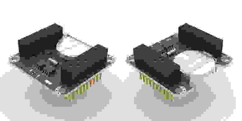
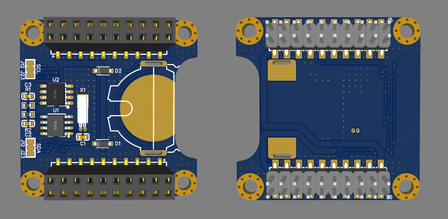
RTC_PCF8563 module
Why do you need a separate real-time clock module at all, since the RTC is already in the ESP32-S3? The fact is that in the official WROOM-1 modules there is no separate pin for powering the RTC of the battery powered domain. The VDD3P3_RTC pin of the microcontroller on the WROOM-1 module board is connected directly to VDD33.
Why? I don’t know. I assume that there are some hardware problems with the internal RTC.
The module is based on PCF8563 chip with I2C interface. At one time, I chose the RTC chip according to the criterion of availability from an RTC with a supply voltage of 3.3V.
In addition to the RTC chip, the board contains a 32 KB EEPROM chip with an I2C interface. Just in case.
The module uses a slotted CR2032 battery holder, so the battery can be changed without disassembling the modules. During development, I had to try on many different battery holders, because most of them do not fit between the pins of the inter-module connectors. The battery does not go beyond the dimensions of the module, and the rounded milling of the board in the area of the battery helps to replace it.
The module can be installed with the battery facing the front or the back. When turning the module 180 degrees, you need to solder the jumpers J1 and J2 to the appropriate position.

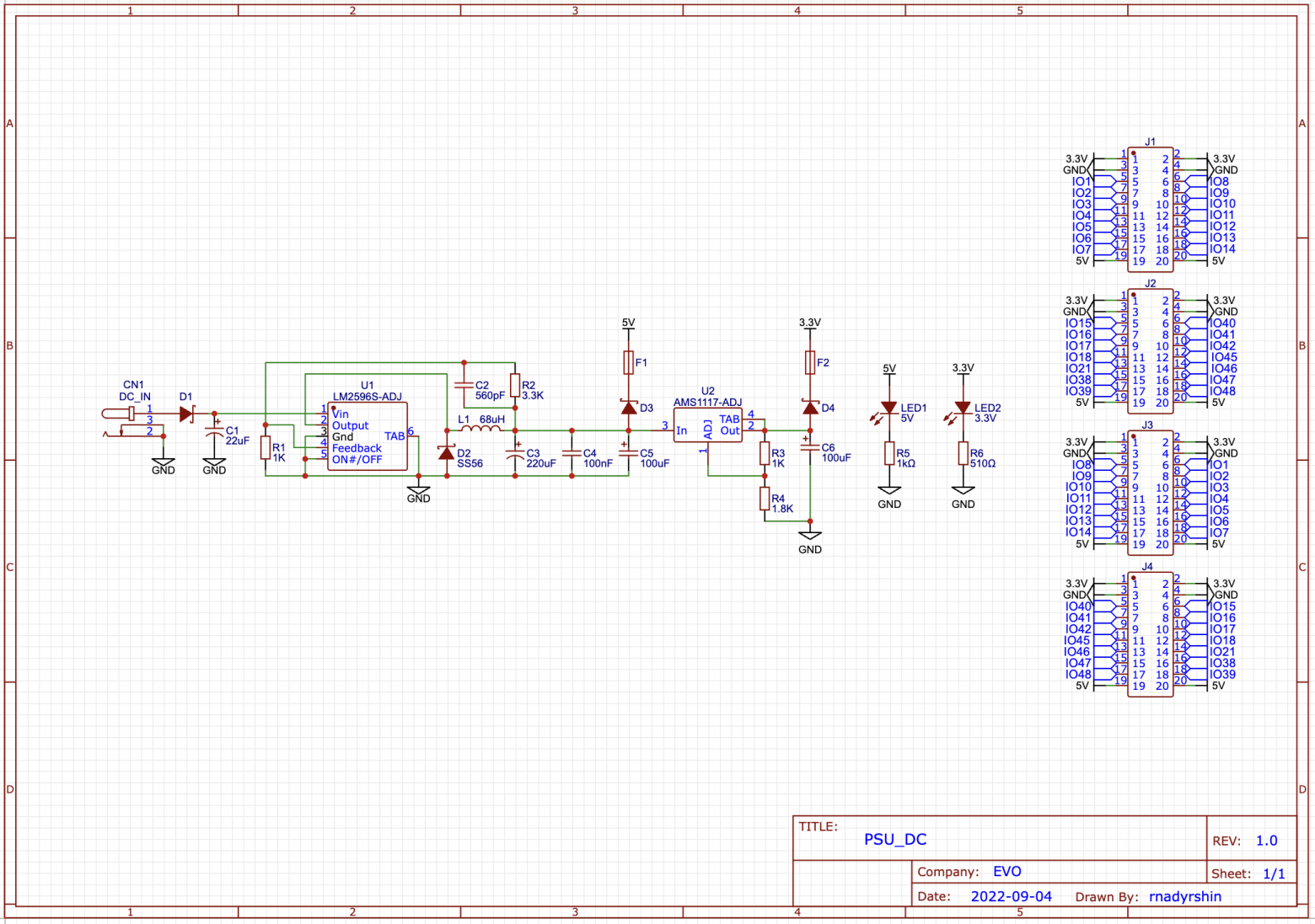
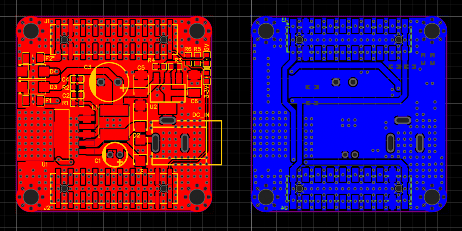
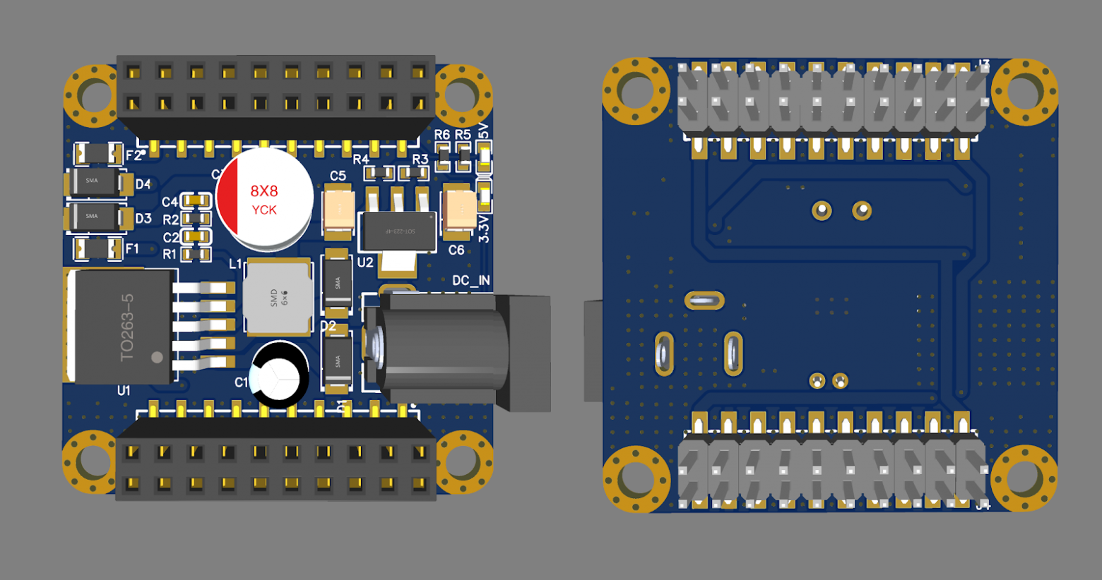
PSU_DC module
The module is powered by an external DC power supply. Input voltage range: 8…45V. There is protection against reverse polarity by a diode at the input.
The input voltage is first reduced to 5V by a pulsed Step-Down LM2596, which is fed into the 5V rail via a Schottky diode (dropping down to 4.8V). The 3.5V voltage is generated by the 1117-ADJ linear regulator and fed through the Schottky diode to the 3.3V bus. Diodes allow you to include in the assembly several power supplies that can be used simultaneously (for redundancy).
There are 2 LEDs on the back right of the module, signaling the presence of voltage on the 5V and 3.3V buses.
A round connector with an outer diameter of 5.5 mm, popular among power supplies, is used.
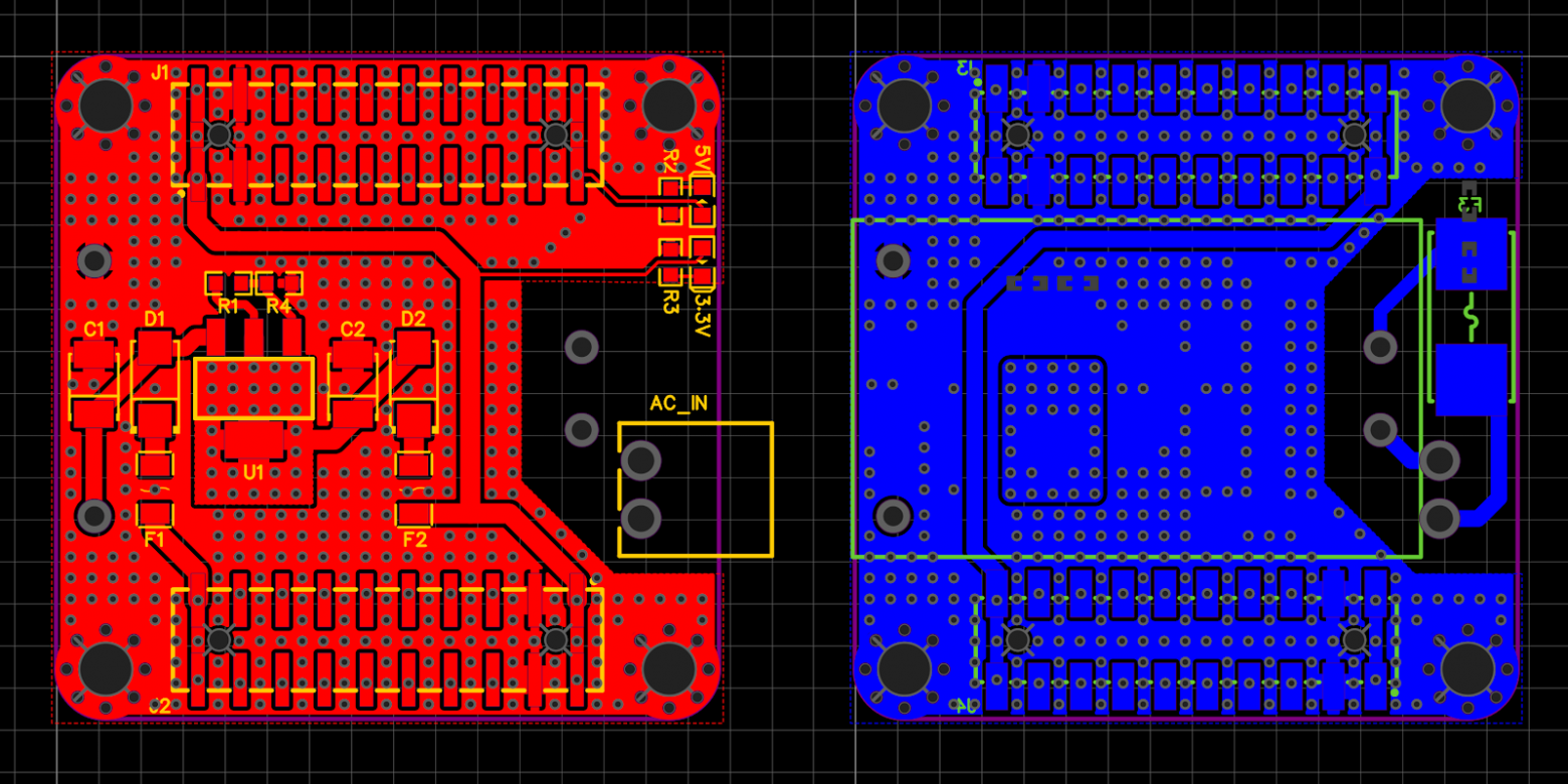
PSU_AC module

The module is an AC power supply. Input voltage range — 100…240V. Power up to 3 W. There is a fuse in the holder at the input.
The 5V voltage is generated using the AC-DC HiLink HLK-PM01, then it is fed into the 5V bus through the Schottky diode (dropping to 4.8V). The 3.5V voltage is generated by the 1117-ADJ linear regulator and fed through the Schottky diode to the 3.3V bus.
The AC-DC is 15mm high and does not fit in the space between 2 adjacent modules. Therefore, the PSU_AC module must be placed at the bottom of the assembly. In addition, it is easier to provide cooling for it in the case and you can try to provide easier access to the fuse.
There are 2 LEDs on the back right of the module, signaling the presence of voltage on the 5V and 3.3V buses.

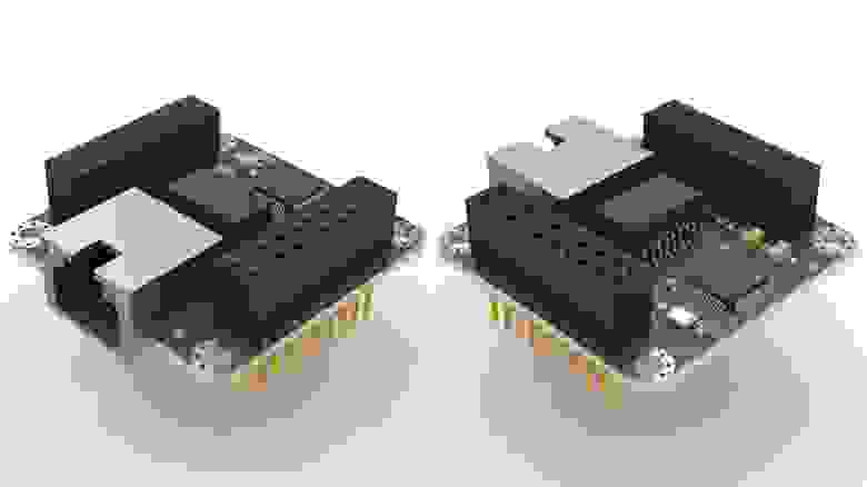
Assembly examples
There are still few ready-made modules and assemblies can also be assembled a little. Let’s take a look…
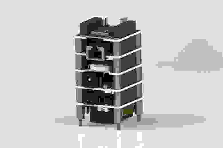
1. CPU_ESP32S3 + PSU_DC
Device based on a powerful 2-core microcontroller with 8 MB RAM, WiFi, Bluetooth LE, 5 RGB LEDs on the front, with a USB-C (Device) port and powered by a wall outlet.
Dimensions: 40×40x43 mm
 CPU_ESP32S3 + PSU_DC
2. CPU_ESP32S3 + ETH_W5500 + RTC_PCF8563 + PSU_DC + PSU_AC
Device based on a powerful 2-core microcontroller with 8 MB RAM, WiFi, Bluetooth LE, 5 RGB LEDs on the front, USB-C (Device) port, 1 Ethernet port, RTC, 32 KB EEPROM and 2 power options (for redundancy) — from an outlet and from a DC source.
Dimensions: 40×40x85 mm
 CPU_ESP32S3 + ETH_W5500 + RTC_PCF8563 + PSU_DC + PSU_AC
3. CPU_ESP32S3 + 2xETH_W5500 + HUB_1×2 + RTC_PCF8563 + PSU_DC + PSU_AC
Device based on a powerful 2-core microcontroller with 8 MB RAM, WiFi, Bluetooth LE, 5 RGB LEDs on the front, USB-C (Device) port, 2 Ethernet ports, RTC, 32 KB EEPROM and 2 power options (for redundancy) — from an outlet and from a DC source.
Dimensions: 81×40x71 mm
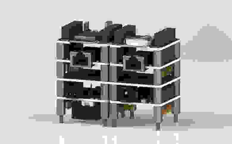 CPU_ESP32S3 + 2xETH_W5500 + HUB_1×2 + RTC_PCF8563 + PSU_DC + PSU_AC
Planned modules
PSU module with 18650 battery (vertical) and charge controller with I2C read status.
Radio modules: RF up to 1 GHz, NRF24, LoRa, GSM, GPS, etc.
Modules with various sensors.
Modules for industrial interfaces: CAN, RS232, RS485, etc.
Modules with discrete inputs/outputs.
Modules with analog inputs/outputs for voltage/current.
Modules with small OLED and IPS displays on the front.
Modules with buttons or joystick on the front side.
Hubs of different sizes.
Finally
I will appreciate any opinion and criticism in the comments.
Now the project is at a stage when the first PSBs have not yet been made, and the development of most modules is still ahead, so almost any errors can still be corrected, and solutions can be improved.
